Thursday, May 26, 2016

Abstract for STEM Showcase on June 8th, 2016


Aaron Buckley and Yu Lin Vivian Tay

Abstract
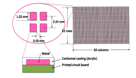
Our topic is creating an affordable 2D multipixel tactile display through electrovibration, which is targeted at visually impaired users who would otherwise have difficulty using a standard display. We create the display through a PCB etching proccess. The convential method for displaying information on digital devices relies upon the sense of vision. Unfortunately, not all people have excellent senses of vision. Those whose vision is impaired are thus unable to experience their devices the same way as others. The tactile display is a concept that allows the visually impaired to use devices by relying on their sense of touch instead. The most common method is to use electrovibration. This is an emerging field so there are very few products on the market. The current products are incredibly expensive and have only a single pixel. Our aim is to use printable circuit boards (PCB) to create an inexpensive alternative multiplex sensation for visually impaired users with tablets devices.

Our goal is to create a series of boards whose configurations are set to specific shapes. This allows us to test out the experience of touching a multipixel display. We first used Photoshop to layout the different patterns for the PCB. Then, we create the PCB boards by using the etching proccess with UV photoresist method on a copper clad board. In the future, we plan to see a minimized multi-pixel display screen that could be attached on a device wirelessly and also allows two fingers to move on the screen at the same time. RepRap.org provided safety guidelines and measurements for the UV photoresist transfer method and referred to procedures on Instructables.com for etching PCBs.

Specials thanks to Mr. Chin Sung Lin for creating this opportunity to research, Ms. Nadya Nikulina and Mr. Peter D’Amico for providing materials and guidiance on the chemical process.

Tuesday, April 5, 2016

Today's In-Class Work

Progress:
Today in class, Aaron and I finished the 12 by 12, 18 by 18 and 24 by 24 PADS and placed them on the canvas which has been modified to the size of the copper clad. Here’s a photo of our layout. 
 

Our next step is to delete the unnecessary wire connections in order to create the patterns. Also, as you can see, there are a lot of wasted space, so I am trying to optimize the surface by placing more pads and move them around. I believe that we will be able to print this layout and begin our etching process on Thursday !

Sunday, April 3, 2016

Progress Report


Since the Steminar presentation, I have realized that using Photoshop may not be the best way to complete the PCB designing. Photoshop is definitely time-consuming since the copy-and-paste function doesn’t work as easily as we thought it should be. Even when we switched to another software, Fireworks, the layers would get weird and messed up. So, now I have been using QCAD to complete the PCB designing. I find the schematics on QCAD really helpful and useful. It definitely made my job a lot easier as well. 

Tuesday, March 22, 2016

Weekly Progress Report - 3/20

Progress
This past week we made some more progress. On Thursday we found out why the voltage drops as it goes across the 1 MΩ Resistor on the breadboard. The right side of the breadboard must be shorted to the ground.

Problem
As previously mentioned, the right side of the breadboard is somehow shorted to the ground. We must figure out how it is shorted to the ground. In addition we need to change it so that it will not be shorted to the ground.

Plan
Figure out how the circuit is shorted to the ground. Change the layout so that it will no longer be shorted to the ground. Test the circuit with the improved layout.  See if the circuit functions properly. If not, continue searching for problems in the circuit.

Thursday, March 10, 2016

Standard Trace Width

http://www.expresspcb.com/tips-for-designing-pcbs


Found it!!

"A good trace width for low current digital and analog signals is 0.010″.
Traces that carry significant current should be wider than signal traces. The table below gives rough guidelines of how wide to make a trace for a given amount of current.
0.010″ 0.3 Amps
0.015″ 0.4 Amps
0.020″ 0.7 Amps
0.025″ 1.0 Amps
0.050″ 2.0 Amps
0.100″ 4.0 Amps
0.150″ 6.0 Amps" 

Thursday, March 3, 2016

Small Update


In the photo above, it shows the new pixels design. It's 12 columns by 12 rows. The shape will be a "U" with a straight line on the top.

I have also created a spread sheet to find our ideal trace dimensions since we do not have most information to use the trace width calculator.

Thursday, February 4, 2016

Progress and PCB Layout Wiring


Wiring Calculator

http://circuitcalculator.com/wordpress/?p=25/

We need to find what's the minimum dimensions needed for the wiring when I piece all of the patterns together. The wires cannot be too thick because that will complicate, or too thin that it won't work.

Updated Layout Pattern

Wednesday, January 27, 2016

Materials


Materials
Where to Get
copper clad 20cm x 15cm
done
transparencies
done
hydrochloric acid
done - d’amico
hydrogen peroxide
done - d’amico
photoresist developer
amazon- product link
acrylic waterproof black ink
amazon - product link
small drill bits
0.25 mm - 1.15 mm
0.3 mm - 1.2 mm
amazon - product link
handle driller
done?
plastic container (small size, small enough for the board)
a clean tooth brush
done
rubber gloves
school lab
a timer
done


Thursday, January 21, 2016

In Progress PCB Layout (Re-do)


Next step: Wire the pixels, making sure the wire is not too thin.

Conversions
MM --> INCHES

1.02 mm = 0.04"
0.5mm = 0.019685"
2.54mm = 0.1"
5.58mm = 0.22"
10mm = 0.393701"
2.21mm = 0.08700787"

Saturday, January 16, 2016

Similar Idea

Interesting...

https://www.yahoo.com/tech/researchers-develop-braille-kindle-blind-160115335.html

Friday, January 15, 2016

Thursday, January 14, 2016

Procedure for PCB

Procedure for creating a PCB with etching.

  1. Procedure Etching a one-sided PCB
    1. Print the bottom side layer PCB layout on a transparency
    2. Wash hands to remove oils from hand, do not touch the laser printer with your fingers. Also keep the pages as flat as possible
    3. Remove packaging from copper clad and make sure you do not touch the surface of the copper clad either because of the same reason from above
      1. You can cut the copper clad to a small strip for testing
      2. Use a slightly damp paper towel to clean off residual dust
    4. Place the copper clad on a flat, strong and heat resistant surface. Set up a clothing iron to the hottest setting (Linen usually has the highest temperature)
    5. Make sure the copper side of the clad is facing up and the blank is facing down. Align the transparency with the toner facing toward the copper side). Do not move the transparency
    6. *CAUTIONS* Press hard on the iron on the transparency, which is on top of the copper clad
    7. Hold the iron on the same spot for one whole minute and make sure the pressure on the copper clad is hard
    8. For five more minutes, slowly remove the iron but make sure that the paper will not slide on the copper. Leave the cooper clad on the table until it is fully cool down. This is allowing the toner to stick to the copper and prevent getting burns
    9. After the copper clad is cooled down, place the board in a bucket of cold water and soak for about five minutes. Try to peel the transparent from the board, so that only the toner will leave on the copper clad.
    10. If you find the copper clad and the toner ink are misaligned, you can use lacquer thinner and paper towel to clean the toner from the copper clad and redo the procedure


    Part 2

    1. Make sure you are at a ventilated place with windows or a fan while you complete the following steps.
    2. Pour 2 cups of hydrogen peroxide to a plastic container
    3. Carefully pour 1 cup of Muriatic acid, these are the steps for creating the etching solution
    4. Make sure that you don’t use any metal containers or stainless steel sinks as tools with this mixture, that would add aggressively etch metal .
    5. Add the Acid
    6. Place the copper side up of the board in the plastic container with the homemade etching solution
    7. Use a soft plastic brush to wipe the board. The copper will begin to dissolve
    8. It will take about 5 minutes to get all the exposed copper dissolved.
    9. If you leave the copper clad for too long in the etching mix, the traces will dissolve under the toner that is supposedly protecting them
    10. *Put on rubber gloves* Carefully take the board out of the etching solution amid rinse the board under warm water for about 1 minute. Wash it clean and dry the board with a paper towel
    11. The solution should be used up because the copper have been dissolved within the liquid. Throw away the solution by diluting it in a 5-gallon pail of water. The acid level and the copper content will be decreased.
    12. If you intend to add ground planes on your board, use less etchant when you are making smaller sized boards
    13. Use lacquer thinner and paper towels to remove any toner left on top of the copper traces. This is to help the copper form oxidizing.
    14. Drill all holes through the through-hole parts using your choice of PCB drill bits and rotary tools.